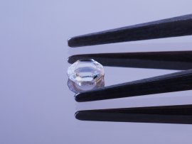
 A high-purity single-crystal diamond made at Fraunhofer IAF. Credit: Fraunhofer IAF
Synthetic diamond crystals are of interest to many industrial sectors. Their unique properties make them a suitable material for numerous applications including lenses for high-energy laser optics, X-ray radiation detectors and ophthalmological scalpels. Fraunhofer scientists produce artificial diamonds in all shapes and sizes ranging from discs to three-dimensional shapes and even hollow spheres.
Diamonds are highly sought after as jewelry and as a form of capital investment. They are also prized by the research community, but not because of their brilliance or symbolic significance – it is their physical properties that make these gems precious to scientists. Diamonds are extremely hard, have unrivaled thermal conductivity and have a broadband spectral transparency that stretches from ultraviolet to far infrared, making them the ideal material for a host of different applications. Consequently, there is a large market for synthetic diamonds: they can cut through steel as if it were paper, dig their way through the earth on the tips of drilling heads, are used as scalpels in operations and can act as bio-electrochemical sensors for detecting substances such as DNA.
Researchers at the Fraunhofer Institute for Applied Solid State Physics IAF in Freiburg make synthetic diamonds of the highest quality. They produce three-dimensional geometries and discs of different diameters and thicknesses using plasma-enhanced chemical vapor deposition (CVD), a process by which diamond is chemically deposited on a substrate from the gas phase. A specially pretreated silicon or silicon dioxide (silica) substrate is coated with diamond by means of microwave plasma in an ellipsoidal reactor. Fraunhofer IAF's diamond laboratory contains eight such plasma reactors for growing diamonds in polycrystalline (that is, made up of countless smaller crystals) and single-crystal form. Scientists can determine the orientation of polycrystalline diamond growth by applying small diamond seed crystals to the substrate before plasma deposition occurs. Single-crystalline diamonds with a continuous homogenous crystal lattice structure, however, have to be grown on a single-crystal diamond substrate. "We use chemical vapour deposition because it allows us to coat larger substrates, unlike other manufacturing processes such as the high pressure high temperature method. What's more, this method will enable us to produce diamonds of high enough quality for use in electronic applications, and means we can homogeneously deposit diamonds with diameters of up to 10 cm on silicon substrates, " states Nicola Heidrich, group manager at Fraunhofer IAF. But making diamonds requires patience: a 100-nanometer-thick poly- or nanocrystalline layer can be grown within an hour; single crystals grow at a rate of up to 20 micrometers an hour.
YOU MIGHT ALSO LIKE


